555 Circuits Part 2
A second collection of the 555 RC oscillator to produce voltage multiplier circuits
Continuing on from our first look at the operation of the 555 timer, this second tutorial about the 555 Timer looks at some practical uses and circuits we can build when using the 555 as an astable multivibrator.
We recall from the our previous tutorial about the 555 timer that to get it to oscillate as a square-wave oscillator we need to continuously retrigger it with the timing period, T and therefore output frequency, ƒ being set by the timing capacitor C and feedback resistors RA and RB. The duty cycle, D as well as the frequency is controlled by the ratio of these timing resistors.
With that in mind, we can design our basic 555 multivibrator to give us an output frequency of about 1500 hertz using preferred component values as shown.
Basic 555 Multivibrator Circuit
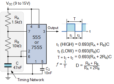
Using the component values given will produce values of: t1 = 375uS, t2 = 325uS, T = 700uS, ƒ = 1430Hz or 1.43kHz and a duty cycle, D of about 0.535, or 53.5%.
Note also that as the duty cycle is 53.5%, when the 555 astable oscillator is connected to a supply voltage of 9 volts, the average output DC equivalent voltage present on the output, pin 3 will be: 9*0.535 approximately equal to 4.8 volts, and when connected to a supply voltage of 15 volts, the equivalent DC output voltage will be 15*0.535 which equals about 8 volts. This voltage level represents the DC input voltage (VIN to the connected voltage multiplier circuit.
555 Voltage Multipliers
Transformers are very efficient devices for converting an AC primary input voltage to a secondary output voltage, either stepping the secondary voltage up or down with respect to the primary. But what if we wanted to convert a steady state DC voltage from one value to another, then we can not uses transformers for this.
The 555 timer can be used to convert a DC voltage to a much higher DC voltage, and even reversing the polarity of a DC voltage with just a few additional components added to its output pin. Many electronic applications require different low-current voltage supplies to power different parts of a circuit with the simple 555 oscillator above configured as a transformerless DC-to-DC voltage multiplier used to satisfy many of these low-power applications.
555 Voltage Doubler Circuit
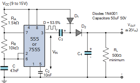
The most basic and easily constructed DC-to-DC voltage multiplier is that of the voltage doubler. The 555 is configured as an astable multivibrator to supply the input conditions for the “charge pump” circuit created using the diode and capacitor network as shown.
555 Voltage Doubler Circuit

This simple 555 voltage doubler circuit consists of a 555 oscillator and a single capacitor-diode voltage doubler network formed by C3, D1, D2 and C4. This voltage doubler circuit multiplies the supply voltage and produces an output that is approximately twice the voltage value of the input voltage minus the diode voltage drops.
When the output at pin 3 is LOW, the 50uF capacitor (C3) charges up to the supply voltage through diode, D1 with diode D2 off. When the output from the 555 goes HIGH, the voltage across C3 discharges through diode D2, as D1 is reverse biased, adding its voltage to the source voltage as VCC and C3 are now like two voltage sources in series.
The timing cycle from the 555 changes state again from HIGH to LOW and the cycle repeats once again, thus producing a DC load voltage which is twice the original input voltage, that is a multiplication factor of two (voltage doubler). Then a 555 voltage doubler circuit can produce an output voltage from about 10 to 30 volts at very low current.
Another point to note is that the frequency of oscillation of the 555 astable multivibrator used to generate the square-wave input signal will determine the value of the capacitors used, as they along with the connected load value create a RC charging/discharging circuit to filter the output voltage. Too low a capacitance value, or too low the frequency of oscillation will produce ripples in the output voltage waveform and therefore a lower average DC output voltage.
With no-load connected, the output voltage will be twice the 555’s original supply voltage. The actual output voltage will depend on the value of the connected load, RL and the load current, IL. As given, the 555 voltage doubler circuit above can supply about 30mA at the rated voltage.
There are many variations of the voltage doubler circuit above, but each one uses two diode/capacitor pairs to provide the x2 multiplication factor. By adding or cascading more diode/capacitor networks to the voltage doubler, we can create circuits which can create voltage multiplication ratios as high as we want.
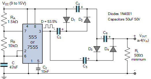
So for example, by adding half a diode/capacitor combination to the 555 voltage doubler circuit creates a voltage tripler circuit with a multiplication factor of x3, and adding a second full diode/capacitor section to the 555 voltage doubler circuit will create a voltage quadrupler circuit with a multiplication factor of x4, and so on as shown.
555 Voltage Tripler Circuit

Voltage quadrupler using the 555 timer by cascading together two voltage doubler networks giving an output voltage of approximately 4VIN if losses and diode voltage drops are ignored.
555 Voltage Quadrupler Circuit
As well as producing voltage multipliers with different positive output voltages, we can also configure them to produce negative output voltages by simply reversing the directions and the polarities of the diodes and capacitors used as shown.
555 Negative Voltage Doubler
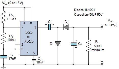
Then we have seen that 555 timer based voltage multipliers can be used to double, triple or even quadruple a single supply voltage to provide various positive and negative output voltages. While in theory there is no limit to the amount of voltage multiplication that can be produced by cascading together multiple diode/capacitor sections to produce progressively higher voltages such as those used in air ionizers or bug zappers. However, care must be taken to ensure against electric shock when dealing with such high output voltages.
555 DC-to-AC Inverter
We can take this idea of a 555 voltage multiplier one step further by using the basic 555 timer circuit to produce a DC-to-AC inverter. With the 555 configured to operate as a square-wave oscillator and a few additional components, we can produce a sine-wave output at the desired voltage level, either 120 volts or 240 volts as shown.
555 DC-to-AC Inverter
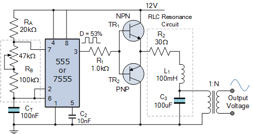
So how does the 555 DC-to-AC Inverter circuit work. The 555 timer is configured to oscillate as an astable multivibrator producing a square-wave output the same as before. This time however we want the output frequency to be the same as the AC mains frequency, that is either 50Hz or 60Hz and this is achieved using a 47kΩ potentiometer.
Timing resistance RB consists of a fixed value resistor of 100kΩ in series with a potentiometer of 47kΩ. When the potentiometer is adjusted so that its wiper is in its zero position, RB = 100kΩ (0 + 100kΩ), and when it is adjusted in the opposite direction to its maximum position, RB = 147kΩ (47kΩ + 100kΩ).
So by using the previous formulas, the output frequency from the 555 can be adjusted using the potentiometer from about 46Hz to 65Hz, providing the required 50Hz or 60Hz output frequencies as we would expect to see from the AC mains supply.
The square-wave output frequency from pin 3 of the 555 is fed via a current limiting resistor, R1 to the bases of two complementary transistors. When the output is HIGH (current source) the NPN transistor conducts and the PNP transistor is OFF, and when the output is LOW (current sink) the PNP transistor conducts and the NPN transistor is OFF. Thus as the square-wave output signal alternates between HIGH and LOW, it switches one or the other transistor as they are complementary pairs.
Transistors TR1 and TR2 can be any reasonable complementary NPN and PNP transistor such as the TIP41, 2N2222 and TIP42, 2N2907 respectively, or a matched Darlington pair such as the NPN TIP140, TIP3055 and PNP TIP145, TIP2955 respectively. The choice of output transistors will depend on voltage and current ratings of the transformers primary winding but ideally it should have a low VA rating.
The complementary output stage of TR1 and TR2 is used to drive the primary winding of a small transformer whose ratio of primary to secondary turns will produce the desired output voltage. However if we were to feed the transformers primary directly from the transistor stage, the output waveform from the transformers secondary winding would be that of a square-wave. Thus as we are building a DC-to-AC inverter, we need some way of converting the 555 timers square-wave output on pin 3 into a sinusoidal shaped waveform from the transformers secondary winding.
The RLC filter circuit connected between the transistor stage and the primary winding acts as an RLC resonance circuit tuned to the required output frequency. However, as we can adjust the output frequency from between 46Hz to 65Hz using the potentiometer, the RLC resonance circuits resonant frequency will not be exact for the 50Hz or 60Hz frequencies, but we can calculate the values for somewhere inbetween.
Using standard preferred component values, the filter network of resistor R2, inductor L1 and capacitor C3 produce an RLC resonance circuit tuned to about 52Hz. The transformers primary winding is connected across the capacitor producing a reasonably sinusoidal waveform on the secondary at the required voltage determined by the transformers turns ratio.
Then we can use the 555 timer to produce a very basic DC-to-AC inverter at the required AC output voltage and frequency, for example 120V at 60Hz, or 240V at 50Hz, from a single 12 volt DC supply with an output wattage rating depending on the output transistor stage and transformer used.
